
Semiconductor Patent Drafting
Semiconductor Patent Drafting Services India
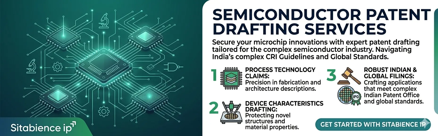
At Sitabience IP, we understand that semiconductor innovation isn’t just about shrinking nodes; it’s about securing the core intelligence that powers the modern digital world. In India’s rapidly evolving semiconductor ecosystem, protecting Integrated Circuits (ICs), fabricated processes, and chip architectures requires more than legal acumen—it demands deep, specialist technical expertise.
We provide comprehensive Semiconductor Patent Drafting Services in India, tailored for chip designers, fabrication units, foundries, and embedded system innovators. Our team transforms complex silicon novelties into robust, enforceable patent assets.
Semiconductor technology represents one of the most intellectually demanding fields for IP protection. Drafting a semiconductor patent application involves managing layers of complexity that generic drafting services often miss:
Circuit Design Protection
Protecting original analog, digital, or mixed-signal circuit designs requires translating schematics into precise, textual descriptions while adhering to the statutory requirements of novelty and inventive step. In India, inventors must also consider the interplay between patent protection for new circuit functionality and the Semiconductor Integrated Circuits Layout-Design Act, 2000 (SICLD Act) which protects the physical topography of the chip.
Hardware-Software Integration (Embedded Logic)
Modern chips are rarely purely hardware. They are ecosystems where hardware and embedded firmware are inextricably linked. The barrier to patentability here lies in drafting claims that define the novel hardware structures and how the software controls them, all while navigating the restrictions on “computer programs per se” under Section 3(k) of the Indian Patents Act.
Fabrication Processes
Protecting the “how” is just as vital as the “what.” Innovations in photolithography, etching, doping, thin-film deposition, and packaging (e.g., Flip-Chip, SiP, 3D ICs) are process inventions. Patent drafting must meticulously detail every novel chemical, physical, or temporal parameter within the fabrication flow, ensuring the process is industrially applicable and distinct from commonplace practices.
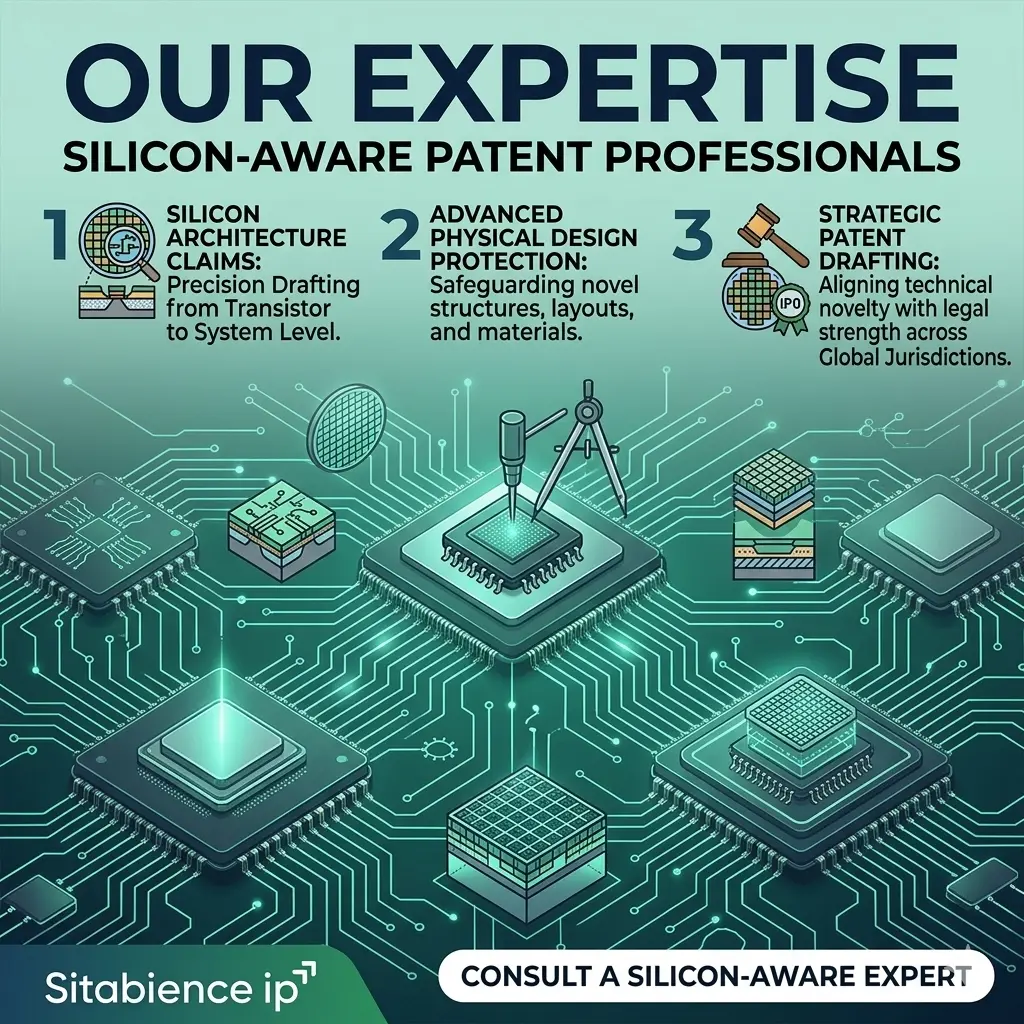
Our Expertise: Silicon-Aware Patent Professionals.
At Sitabience IP, our technical leads hold advanced degrees and have industry experience within the semiconductor domain. We speak the language of engineering, not just the language of law. Our expertise encompasses:
VLSI (Very Large Scale Integration): Expertise in protecting complex digital logic, memory architectures (DRAM, SRAM, Flash), standard cell design, and Power, Performance, and Area (PPA) optimizations.
Embedded Systems: Securing microcontrollers, microprocessors, DSPs, SoC (System-on-Chip) designs, and the critical interface logic between silicon and external hardware.
Chip Architecture: Protecting novel instruction set architectures (ISA), bus protocols, interconnect strategies (e.g., Network-on-Chip), accelerators for AI/ML, and heterogeneous computing models.

Ready to turn your innovation into lasting impact?
Let’s talk AI Patent Drafting Experts that works for you

Engineering Enforceability.
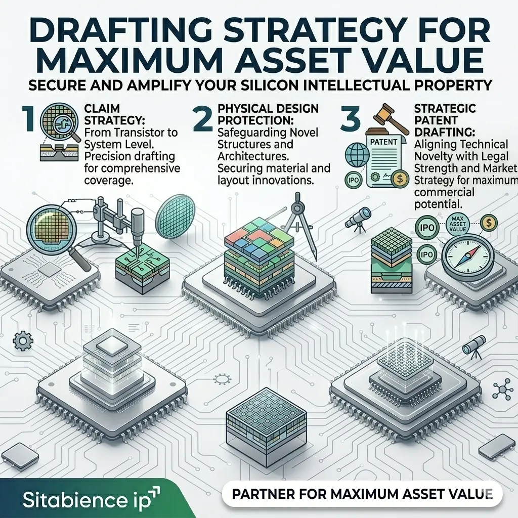
Drafting Strategy for Maximum Asset Value
A weakly drafted semiconductor patent is merely expensive paper. Sitabience IP employs a strategic methodology designed to maximize the commercial value of your silicon IP portfolio in India and globally:
Technical Depth: We conduct exhaustive technical interviews with your inventors to uncover the core novelty of the innovation. We translate raw schematics and process flows into highly detailed specifications that can withstand rigorous examination by Patent Examiners in India, the US, or Europe.
Broad Claims Strategy: We utilize hierarchical claim structures. Starting from the broadest patentable concept, we sequentially narrow the scope through dependent claims. This ensures that while we aim for maximum protection, we also build a layered defense that protects against potential prior art challenges.

our testimonial
What customer say
about our services

Testimonials

Blog / Post
Intellectual Property insights, updates and Trends

Need Help With Patent OR Trademark Registration?
Get in touch with us
Trusted by Innovators Across India and Beyond
- 200+ patents and trademarks filed in the last year
- 98%+ grant success rate in patent applications
- 15-days average turnaround for filing-ready drafts
- 010+ startups and businesses advised on IP strategy